What Clients Say?
Here are testimonials from clients..
How to Prevent Insulation Failures in High-Voltage PCB Designs
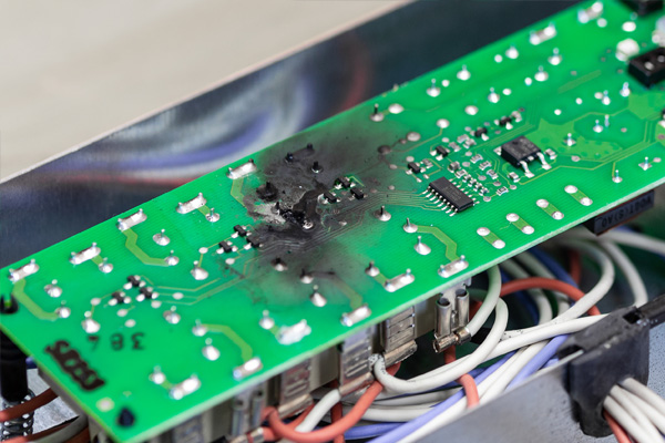
PCB insulation breakdown is one of the most dangerous and costly failure modes in high-voltage hardware. These issues often pass early tests, only to cause catastrophic field failures—from arcing and shutdowns to burned boards and warranty returns. Whether it manifests as a blown fuse, carbonized board, intermittent arcing, or a total product shutdown, insulation breakdown tells you one thing: the board wasn’t designed to handle the real-world voltages and stresses it encountered.
At SOENCO, we’ve seen what happens when insulation strategies are treated as box-checking exercises rather than engineering disciplines. This blog breaks down the most common real-world causes of PCB insulation breakdown, the design pitfalls that lead to them, and how you can prevent these failures long before your product hits the market.
1. Underestimating Real-World Voltage Transients
Many designs pass internal QA but fail in the field because the real-world voltage environment is more complex than anticipated. Common examples include transient spikes, cross-channel coupling, or misinterpreted "working voltage" definitions that underestimate the worst-case scenario.
We’ve seen failures in industrial power supplies that were designed for 400V RMS input but neglected to account for lightning surges on the mains. Another common case: DC/DC converters that assumed 12V rails but saw spikes up to 60V during hot-swapping or inductive load changes.
Key design tips:
• Use surge and transient analysis tools to map out the full voltage range your board might see.
• Apply IEC 61000-4-5 and 60664-1 as relevant for surge immunity and insulation coordination.
• Don’t treat your nominal voltage as your worst-case—design with derating.
2. Creepage, Clearance & Altitude: The Hidden Variables
No surprise here: this is the leading technical contributor to breakdown. But it’s not just about following IPC-2221 tables—real failures happen when designers ignore pollution degree, altitude effects, or board contamination during assembly.
In one case, a customer’s board failed HIPOT testing at 2kV due to solder flux residue bridging a seemingly adequate creepage path. In another, altitude-related derating wasn’t considered on a system deployed at 14,000 feet, and insulation breakdown occurred despite meeting IPC-2221A tables on paper.
Key design tips:
• Adjust clearance and creepage for pollution degree (e.g., conformal-coated boards = PD2).
• Factor in altitude using appropriate standards (air is a weaker insulator above 2000m).
• Use slots or routing to extend creepage where space is tight.
3. Flux, Fibers, and Failures: The Hidden Conductive Paths
Flux, oils, dust, and fiberglass fibers may seem harmless—but under high voltage stress, they form leakage paths or arc points. One of the most subtle (and dangerous) field failures we saw involved a conformal-coated board where fibers were trapped under the coating, eventually carbonizing and forming a conductive path.
Real field story: A customer’s outdoor sensor node began failing intermittently after months in a marine environment. Post-failure analysis revealed condensation mixed with uncleaned flux residues, creating just enough conductivity to start carbonizing the FR-4 substrate.
Key design tips:
• Mandate post-assembly cleaning for all high-voltage boards.
• Avoid rework in critical insulation areas—or re-clean thoroughly afterward.
• Use UV inspection to verify conformal coating coverage.
• Use coating-compatible masking to protect connectors and test points.
4. Why Conformal Coating Doesn’t Guarantee Insulation Safety
Conformal coating isn’t magic—it protects against humidity and contamination, but it’s not a replacement for physical clearance and creepage. We’ve seen several cases where coating was used to justify reduced spacing, only to fail under sustained voltage stress or poor application.
In one case, a silicone coating trapped bubbles between two high-voltage nodes. Those bubbles eventually became the site of partial discharge, leading to tracking and arcing across the board.
Key design tips:
• Never rely solely on coating to make up for insufficient spacing.
• Consider potting instead of coating if you need higher dielectric strength and mechanical support.
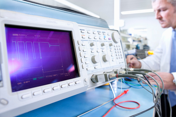
5. Bad Testing = Good Luck, Not Good Design
Some of the most damaging insulation breakdowns come after a unit “passed” testing—because the testing wasn’t consistent with real-world usage. We’ve seen failures where in-house HIPOT used 500V for 1 second, while field use hit 2kV transients regularly. Or cases where only one polarity was tested, leaving vulnerabilities untested.
Real example: A power supply passed all internal testing, but began failing in end-user systems. Turns out, the customer grounded the negative rail during testing—while the internal team had floated it. This exposed an insulation gap near the primary-secondary barrier.
Key design tips:
• Align your compliance testing with actual system usage—including grounding, polarity, and dwell time.
• Perform long-duration insulation resistance testing in addition to HIPOT.
• Track failures across production lots—field failures may only appear after months.
Conclusion
PCB insulation breakdown isn’t just a spec issue—it’s a system-level failure that usually reveals deeper blind spots in design, process, or testing assumptions. These failures aren’t random—they’re predictable and preventable if you know what to look for.
At SOENCO, we help engineering teams build high-voltage PCBs that survive the real world—not just the lab. From creepage and clearance reviews to insulation coordination and failure analysis, we’ll help you catch weak points before they cost you.
Let’s design it to pass, not just to test.
Contact us today to review your insulation barriers, test strategy, or product safety roadmap.
Here are testimonials from clients..

Contact us now for immediate support!